
材料科学とナノテクノロジーにおける走査型電子顕微鏡の役割
The Role of Scanning Electron Microscopes in Material Science and Nanotechnology
Unmatched Imaging Capabilities: Revealing the Micro and Nano World
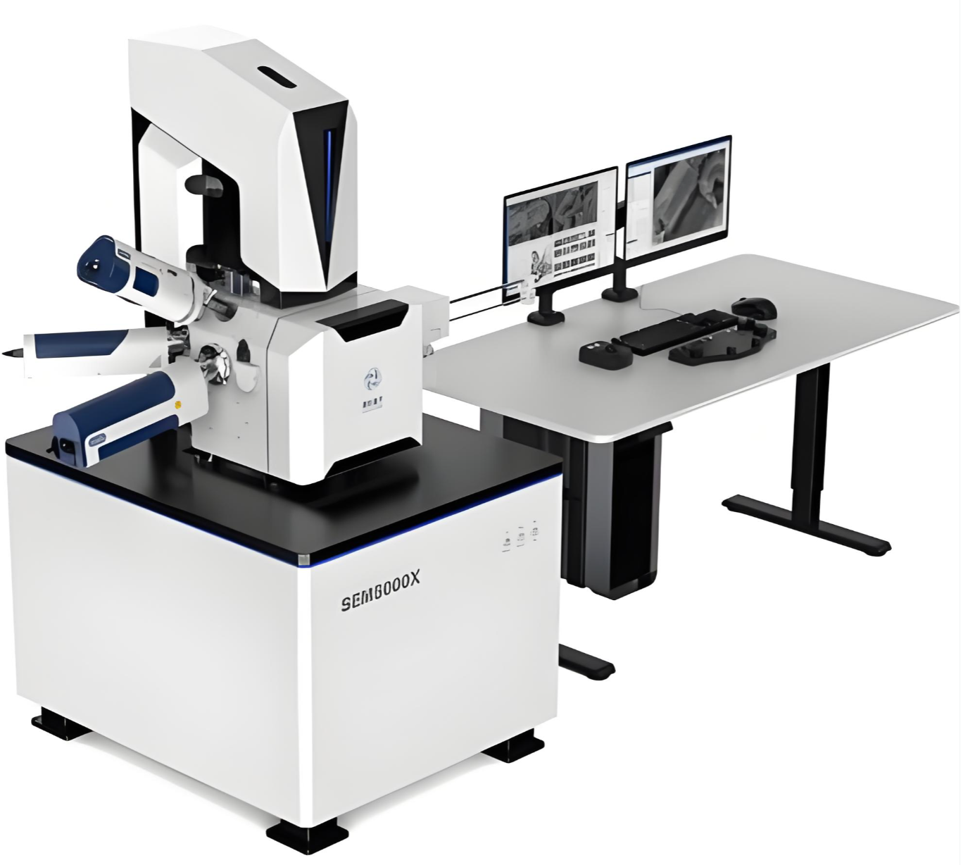
The Scanning Electron Microscope (SEM) stands as a cornerstone instrument in material science and nanotechnology, primarily due to its unparalleled imaging capabilities. Unlike optical microscopes limited by light diffraction, SEM utilizes a focused beam of high-energy electrons scanned across a specimen's surface. The interaction between these electrons and the sample generates various signals, including Secondary Electrons (SE), which are most commonly used for imaging. SE imaging provides exceptional topographical contrast and spatial resolution down to the nanometer scale (typically 1-20 nm), allowing researchers to visualize surface textures, grain boundaries, particle morphology, and microstructural features with breathtaking clarity. This deep, three-dimensional-like view of surfaces is indispensable for characterizing everything from fracture surfaces in metallurgy and the layered structure of composite materials to the intricate architecture of nanoparticles and the precise patterning of semiconductor circuits. The ability to image at these magnifications (from 10x up to 1,000,000x) makes the SEM an essential tool for visualizing the very building blocks and defects that dictate material properties and device performance.
Beyond Imaging: Elemental Analysis and Advanced Characterization
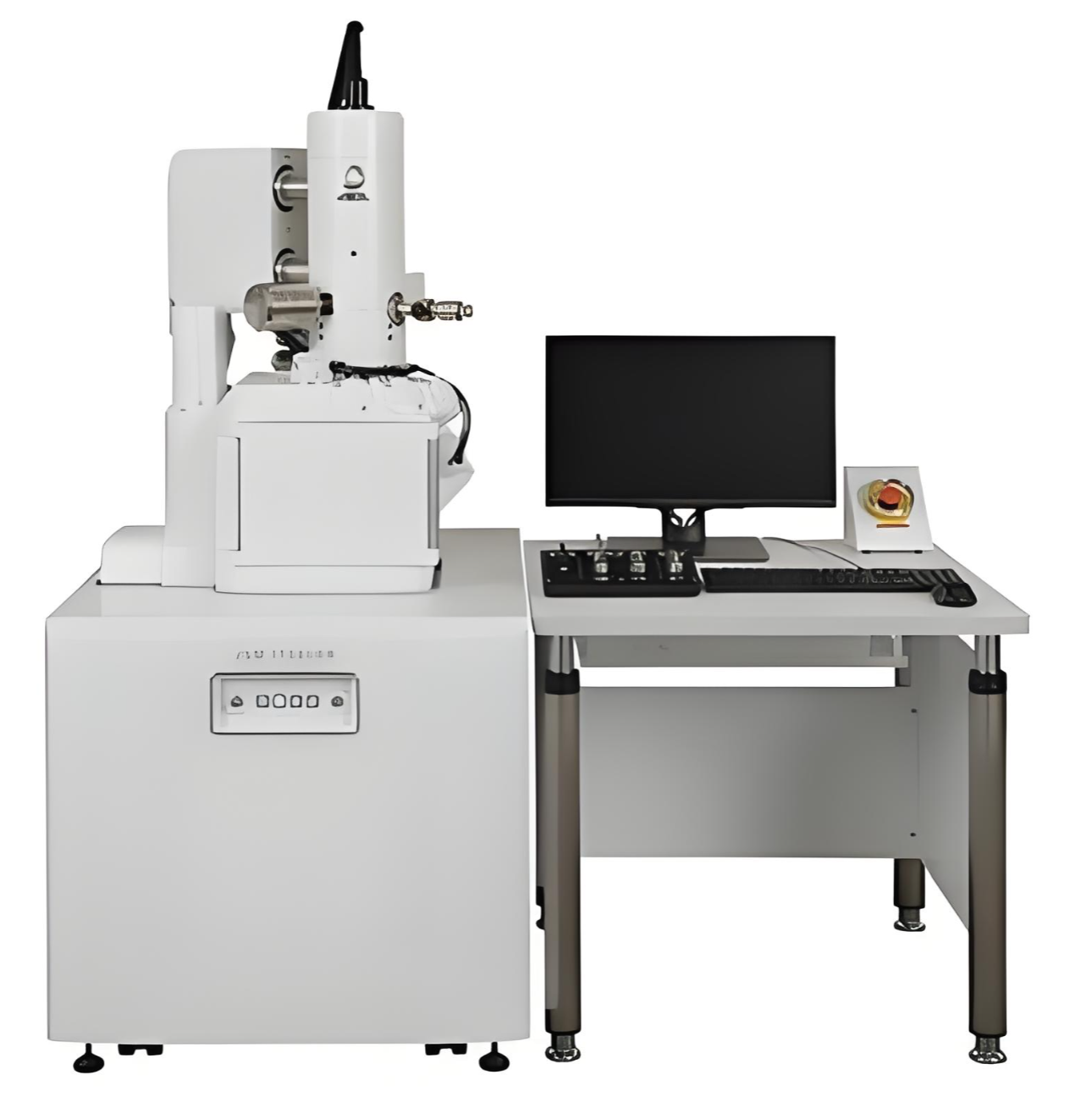
The power of the SEM extends far beyond mere high-resolution imaging. By detecting the Backscattered Electrons (BSE) and characteristic X-rays emitted during electron-sample interactions, the SEM transforms into a powerful analytical tool. Backscattered Electron Imaging provides atomic number contrast (Z-contrast), where brighter areas correspond to elements with higher atomic numbers. This allows for the easy distinction between different phases in a material, such as identifying inclusions in a metal matrix. The most significant analytical leap comes with the integration of Energy Dispersive X-ray Spectroscopy (EDS or EDX). An EDS detector captures the characteristic X-rays, enabling qualitative and quantitative elemental analysis of microscopic features. Researchers can pinpoint the elemental composition of a specific grain, a contamination spot, or a thin coating, mapping the distribution of elements across a sample surface. This combination of high-resolution imaging with in-situ chemical analysis is critical for solving complex materials problems, such as identifying the cause of corrosion, verifying the purity of synthesized nanomaterials, or analyzing the composition of failure sites in electronic components.
Driving Innovation in Nanotechnology and Advanced Materials Development
In the realms of nanotechnology and advanced materials engineering, the SEM is not just an observational tool but an active driver of research, development, and quality control. It enables the ナノ材料の正確な特性評価ナノ粒子のサイズ分布の測定、ナノチューブやナノワイヤのアスペクト比の評価、医療やエネルギー用途のナノ構造スキャフォールドの多孔性の評価など。薄膜技術や半導体製造においては、SEMは極めて重要な役割を果たします。プロセス管理と欠陥レビューリソグラフィパターンや層厚を検査し、デバイスの歩留まりを低下させる可能性のあるサブミクロンの欠陥を特定します。さらに、次のような高度なSEM技術により、電子後方散乱回折(EBSD)結晶構造情報を提供し、粒方位と相分布をマッピングします。これは、強度、導電性、磁気挙動といった材料特性の理解と最適化に不可欠です。Skyline Internationalのようなサプライヤーが提供する信頼性の高いSEM技術と専門知識を活用することで、研究開発チームや品質管理ラボは自信を持ってイノベーションを推進し、新しい材料設計を検証し、製造上の問題を解決し、マイクロスケールおよびナノスケールにおける可能性の限界を押し広げることができます。
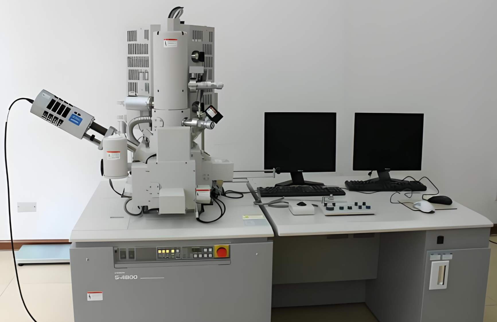
走査型電子顕微鏡(SEM)は、現代の材料科学とナノテクノロジーにおいて欠かせない柱です。マイクロスケールおよびナノスケールの構造をこれまでにないレベルで可視化し、強力な化学分析および結晶構造解析と組み合わせることで、SEMは材料挙動の理解、新製品の開発、製造品質の確保に必要な包括的な知見を提供します。新規ナノ材料の探索を目的とした基礎研究から、ハイテク生産ラインにおける工業品質管理に至るまで、材料の性能を左右する隠れた詳細を明らかにするSEMの役割はかけがえのないものであり、技術・材料開発の最前線で活動するあらゆる組織にとって重要な投資となっています。